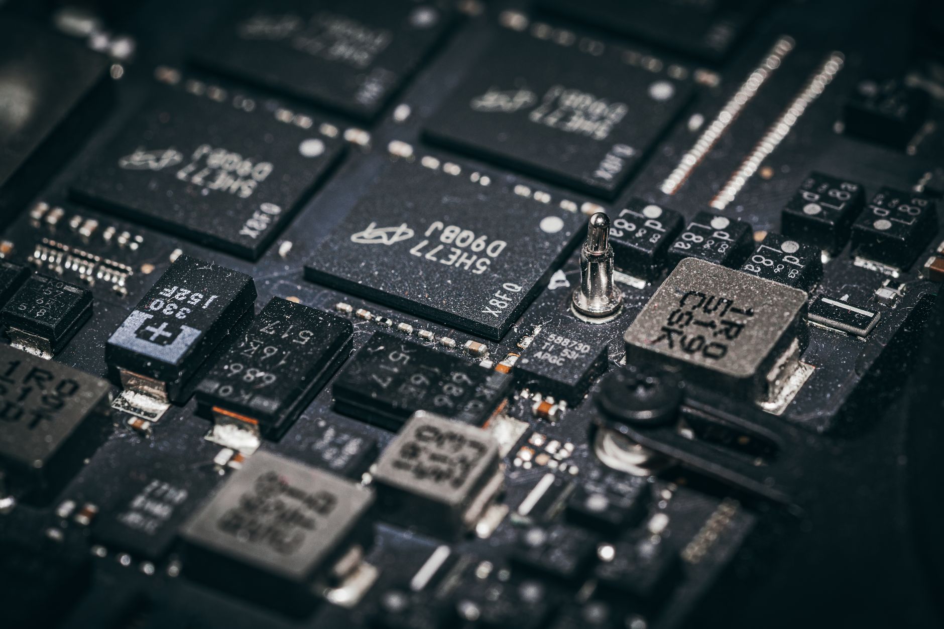
Semiconductor chips are manufactured by building tiny transistors and their electrical connections on a silicon wafer. Factories repeatedly add, alter and remove thin material layers, then test, cut and package the working chips. Each operation must place materials and patterns with extreme precision. The full process takes well over 1,000 steps, and a failure at one stage can leave a chip unusable.
Table of Contents
- Preparing the silicon wafer
- Printing and etching each pattern
- Giving transistors electrical behavior
- Wiring, testing and packaging the chips
- The environmental limits of fabrication
Preparing the silicon wafer
Manufacturing starts by cleaning the silicon wafer so contaminants do not interfere with later steps. The wafer provides a common surface on which many copies of a chip are built at once.
Manufacturers then heat the wafer to about 1,000°C in ultrapure oxygen or water vapor. This forms a uniform silicon-dioxide film that acts as an electrical insulator, according to the Semiconductor Industry Association's March 2026 testimony.
Printing and etching each pattern
photolithography prints a circuit pattern onto the wafer. Machines spin-coat the surface with a light-sensitive material called photoresist, align a mask or reticle, and expose the coating to deep- or extreme-ultraviolet light. A chemical process develops the exposed coating and leaves the intended nanoscale pattern.
Wet chemicals or plasma then etch away material not protected by hardened photoresist. Manufacturers strip off the remaining resist and inspect how accurately the pattern transferred. The wafer can then receive another film and go through another cycle of coating, exposure and etching.
Giving transistors electrical behavior
Patterning creates shapes, but selected silicon regions must also gain specific electrical properties. Manufacturers add controlled impurities through implantation or diffusion, a process called doping. Boron can create p-type regions, while phosphorus or arsenic can create n-type regions.
📨 Get Free News Stories Alerts
Free · No spam · Unsubscribe anytime
Their placement establishes paths that control electron flow through a transistor. Factories also deposit conducting and insulating films ranging from atomic to micron-scale thicknesses. These deposition, doping and patterning operations repeat until the wafer contains its active devices. The Semiconductor Industry Association says completed wafers may contain 8–20 patterned layers or hundreds of layers.
Wiring, testing and packaging the chips
Metallization connects the transistors into working circuits. Manufacturers pattern insulating material and metal—commonly aluminum or copper—to create interconnects between different parts of each chip. Chemical-mechanical planarization polishes each completed layer flat enough to support the next one.
Without that flat surface, later patterns could not be transferred with the required precision. Electrical testing identifies defective die, meaning individual chip units still attached to the wafer. Manufacturers thin and saw the wafer, package accepted die with wire bonds or solder connections, and protect them for shipment, as described in the industry association's manufacturing account.
The environmental limits of fabrication
This precision comes with substantial resource demands. Cleaning, oxidation, deposition, etching and other operations require tightly controlled materials and conditions throughout the fabrication process.
The U.S. Department of Energy's semiconductor supply-chain report identifies high water and energy use, hazardous-waste generation, and fluorinated-compound use as major environmental concerns for semiconductor factories.
You Might Also Like
- How Large Language Models Are Trained
- What a Data Center Draws From the Power Grid
- How Credit Scores Are Calculated